.

Advanced PCB design to cope with the problems of lead-free solder alloys
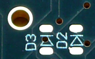


Introduction


As of July 1st. 2006 the RoHS (Restriction of Hazardous Substances) directive became effective. This directive prohibits the use of 6 hazardous materials in the manufacture of various types of electronic and electrical equipment. See the Wikipedia article for more information.

For electronics the most significant effect of this directive is, that now, lead-free solder alloys have to be used for new products. Lead containing solder may still be used for repairs.
I can only encourage the removal of toxic substances out of the environment. However, this does not come without a price:
  • Compared to lead solder, lead-free solder melts at a higher temperature, wets less, does not spread out as good and is more prone to form bridges. These properties affect the soldering process negatively, resulting in more rework after machine assembly.
  • A more important issue of lead-free solder is the growth of whiskers (see Wikipedia) over time. This dramatically reduces the mean time before failure of electronic devices. Whisker growth is in fact the reason why they added lead to solder in the 1940's.
As much as I do care about the environment, I do have my doubts about this and think that more reliable products with lead containing solder, combined with a good recycling program, will be more beneficial for the environment. See here also: Pushback.
Unfortunately, the law is the law.

What to do?


Well, I had three options:
  1. Break the law.
  2. Change the law.
  3. Find ways to minimize these problems.
The first option was out of the question, because if equipment is found, manufactured after July 1st. 2006, containing lead (yes, they do check it at the customs with X-ray fluorescence or LeadCheck), the actions can be anything: Confiscating the product, fines and even jail sentence. I did not want to risk any of these.
The second was considered for a while because I found the magical, scandal filled, lucrative world of politics quite appealing. But, I knew I was just not corrupt enough for that and it would keep me from doing electronics too much.
So, I decided to take the 3rd. option.

Physical mechanisms behind these problems


To be able to find a solution to a problem one must know what the problem is. Thus, I spend of few months of 2008 absorbing knowledge on the following topics: Solder, metallurgy and fluid mechanics.
I could conclude the following:
  • The less wetting, less spreading and bridge forming properties were caused by higher surface tension and less adhesive forces to other metals compared with lead solder. Basically the solder tries to keep together as much as possible by forming a ball (the most energy efficient form of a liquid) and does not wants to spread out much on other metals.
  • Whisker growth is a phenomenon not yet fully understood. Most info I found about it points in the direction of pressure being the main driving mechanism behind it. Metal molecules traveling from regions with high pressure to ones with lower pressure.

How to cope with these mechanisms?


  • Surface tension: Try to keep the solder joints as close as possible to a ball shape.
  • Pressure: Reduce the stress on the solder joints.
  • Quantitative aspect: Quite obvious one: If you look at a SMD component on a typical PCB and scale it to human size, there would be a bathtub of solder on it. Way too much. This can drastically be reduced. The less solder, the less possibility of bridging and the less whiskers. This will also improve the strength of the solder joints. It's the same as with glue: the thinner the layer, the stronger.

PCB wise solutions:


  • Maintaining a ball shape is already being done in BGA (Ball Grid Array) packages. Unfortunately being of no use for low quantity designs and the components I need do not exist in BGA package. The next best thing is using round shapes for the PCB pads. Round pcb pads are closser to a ball than square pads. So, less pull on the surface tension is needed to flow out to the edge of the pads and thus more likely the solder will wet the component. Another benefit of the reduced pull on the surface tension is reduced stress in the solder.
  • Most of the stress on solder joints is generated by bending the PCB. This caused by the heating and cooling down during reflow soldering and by applying force on the PCB. Using a thicker PCB reduces this bending.
  • Reducing the amount of solder is simply done by making the PCB pads smaller. Just big enough for a circumscribed round shape of the component's feet. An extra benefit of these smaller pads is the bigger space between them: Whiskers need to grow longer to become problematic and the problematic directions (the ones in which they reach another joint) for them to grow reduce quadratically with the distance. Also, bridge forming is decreased by increasing the distance compared to the available material to form a bridge.
So what I did was:
  • Create my personal library for my PCB design software of all the components I use, with the shapes optimized for them as described above.
  • Use PCB's double the thickness of original ones. 2.4mm thick FR4 is almost unbendable. SMD components without legs, like capacitors and resistors, are quite sensitive to stress. This protects them too.

Results


Where I used to have 2-3 problems with solder joints on my D80017 modules for runs of 100, before I used this library, There was not a single problem on 100 of the TS-303 MK2 rev2 PCB's. On top of that: the D80017 modules use lead solder, the TS-303 MK2 rev2 lead-free solder and they are a lot more complex.
After that I adapted the D80017 modules to also use this library and the 700 made since then were flawless.

Conclusions


During manufacturing: Using round smaller pads improves the soldering quality beyond anything I expected: 'lead-free-small-round' beats 'lead-big-square'.
Reliability: Whisker growth is a long term effect and I lack the equipment, time and resources to do meaning full tests on this. Time will tell, but the wind in the trees tells me that what I did is quite effective.